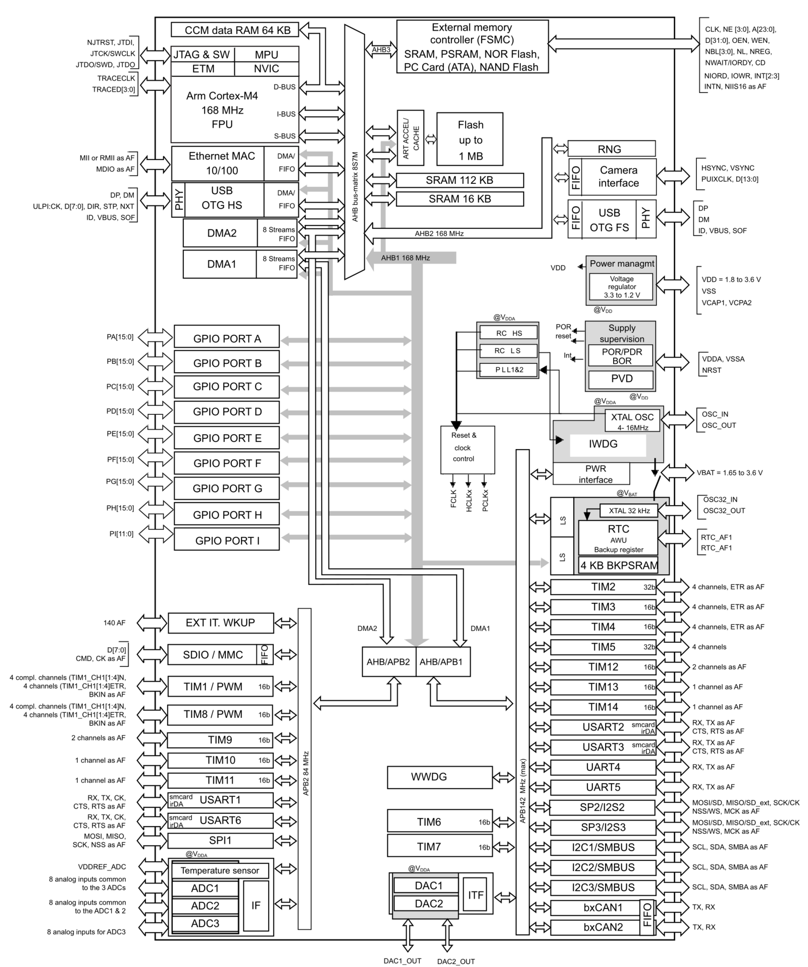
Core Architecture Overview
Core Architecture Overview
The ARM Cortex-M Core
The ARM Cortex-M core implements the ARM architecture, providing the
instruction set and execution pipeline. Key features include:
- RISC (Reduced Instruction Set Computing) architecture
- 32-bit processing capability
- Pipeline stages for efficient instruction execution
- Thumb/Thumb-2 instruction sets for code density
Nested Vectored Interrupt Controller (NVIC)
The NVIC manages interrupts with minimal latency and maximum configurability:
- Priority-based interrupt handling
- Nested interrupt support
- Configurable priority levels
- Dedicated SysTick timer for operating system timing
Memory Architecture
Memory Map
The STM32 uses a unified 32-bit address space with memory-mapped peripherals:
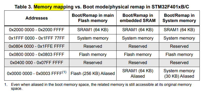
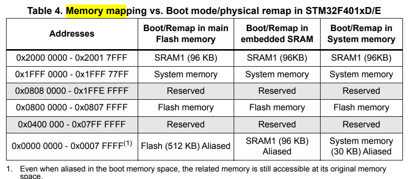
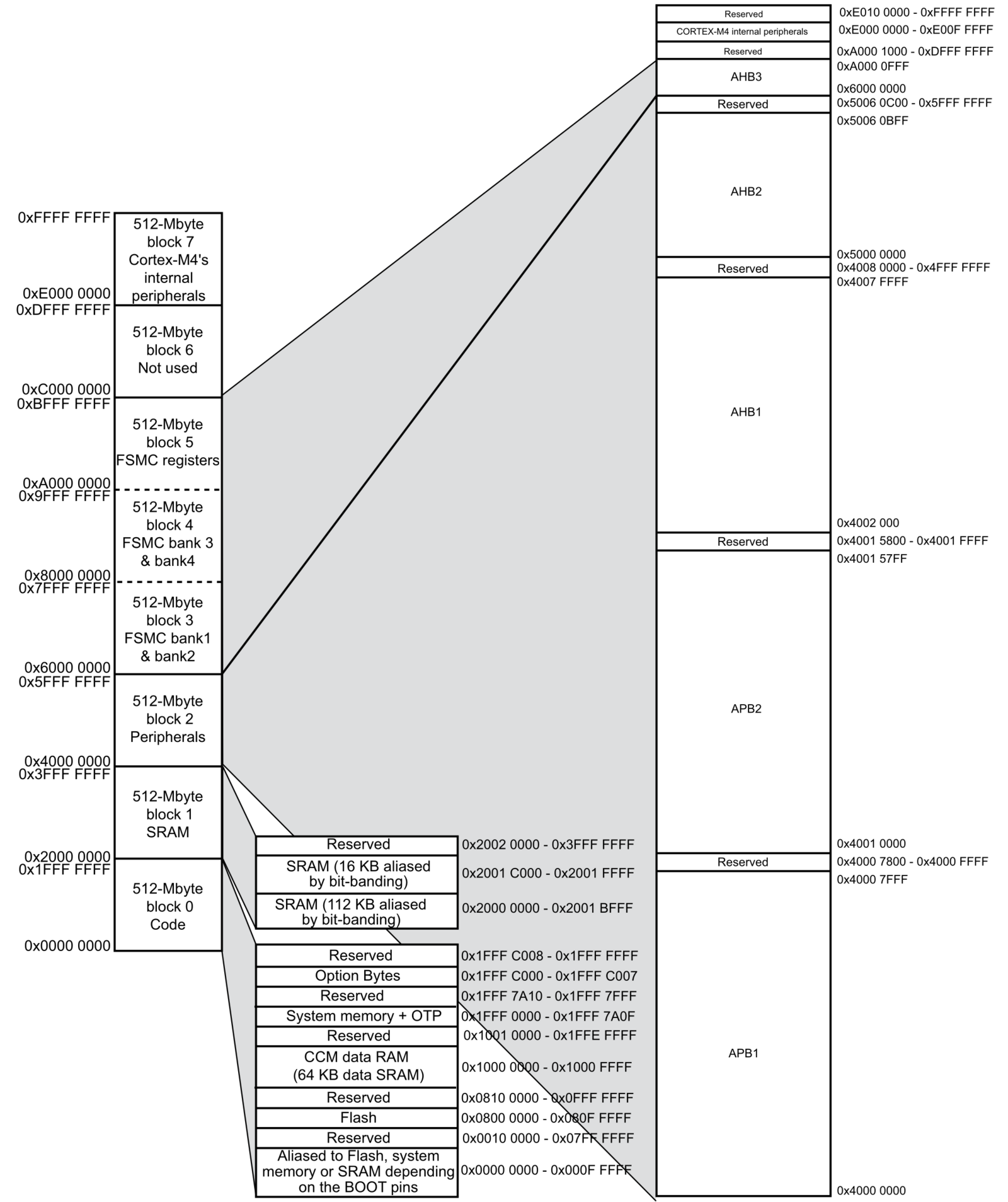
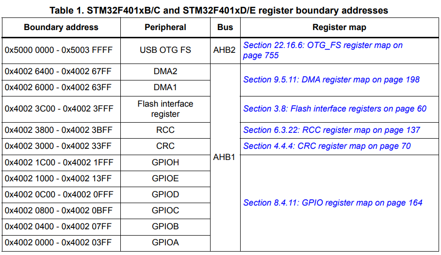
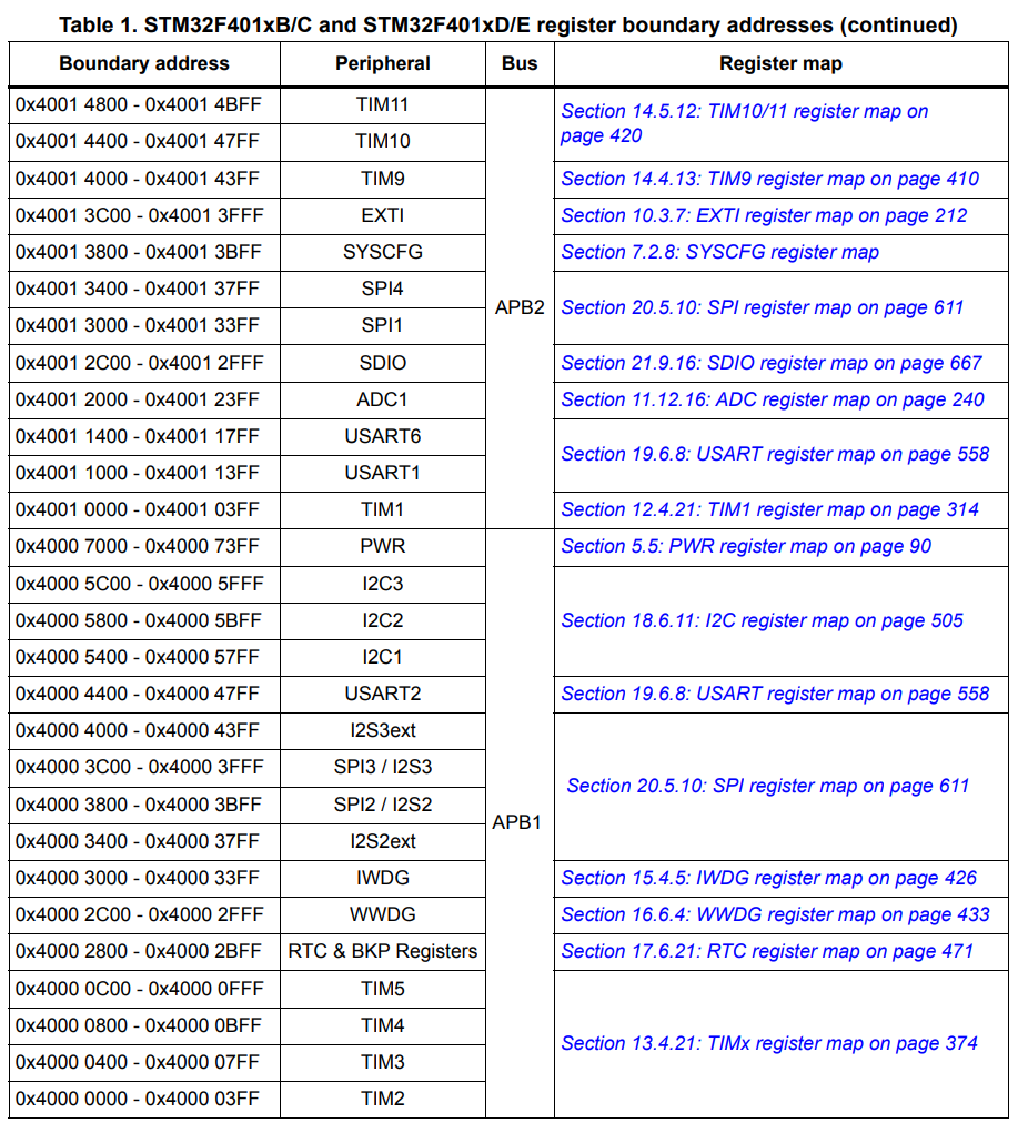
Of these, the most interesting for a new developer are:
-
Flash - 0x8000000
This is where you upload your application.
-
RAM - 0x20000000
This is where dynamic variables are allocated.
Clock System
Clock Sources:
- HSI: High-Speed Internal RC oscillator (typically 8/16 MHz)
- HSE: High-Speed External crystal or clock (4-26 MHz)
- LSI: Low-Speed Internal RC oscillator (32-40 kHz)
- LSE: Low-Speed External crystal (32.768 kHz)
- PLL: Phase-Locked Loop for frequency multiplication
clock tree:
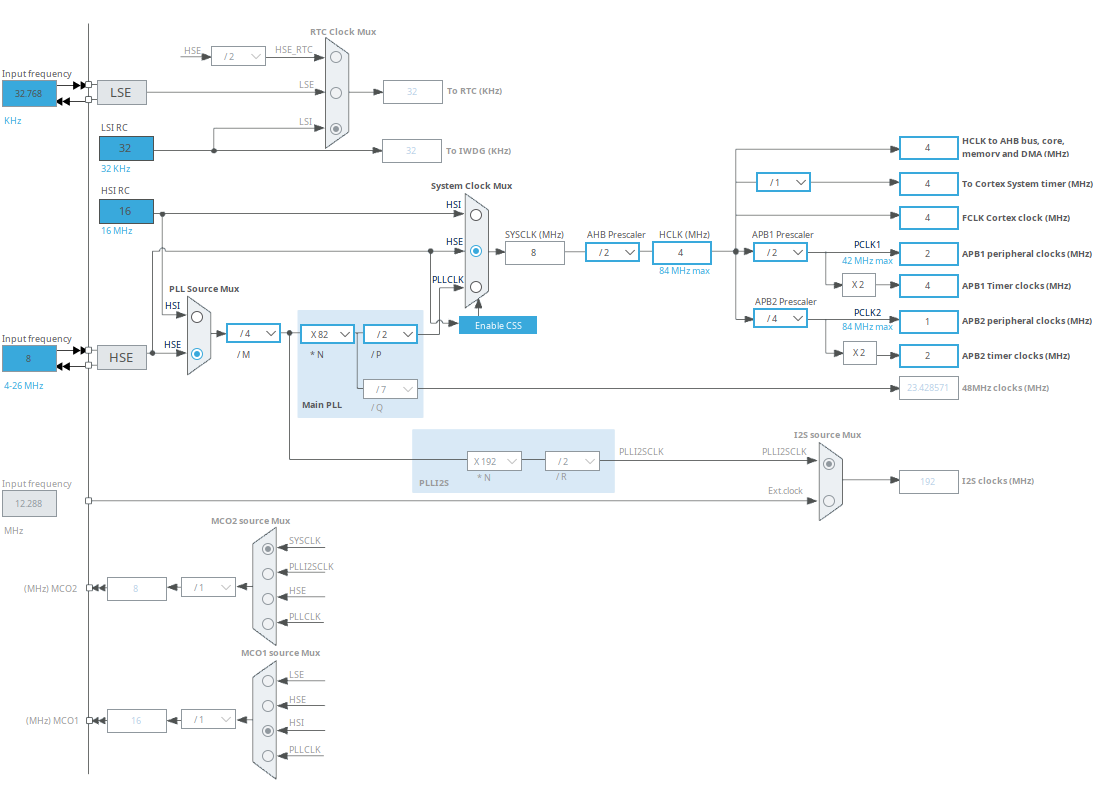
PLL: Phase-Locked Loop.
AHB: advanced high-performance bus
APB: Advanced Peripheral Bus
AHB (Advanced High-performance Bus)
- High-speed system bus designed for fast core components
- Runs at higher frequencies (typically core CPU frequency)
- Connects:
- CPU core
- Flash and SRAM memory
- DMA controllers
- High-performance peripherals (Ethernet, USB)
- GPIO ports
APB (Advanced Peripheral Bus)
- Lower-speed buses for peripheral devices
- Divided into:
- APB1: Lower speed peripherals (I2C, some UARTs, basic timers)
- APB2: Higher speed peripherals (ADC, SPI, advanced timers)
- Connected to AHB via bridge components
- Run at reduced frequencies to save power
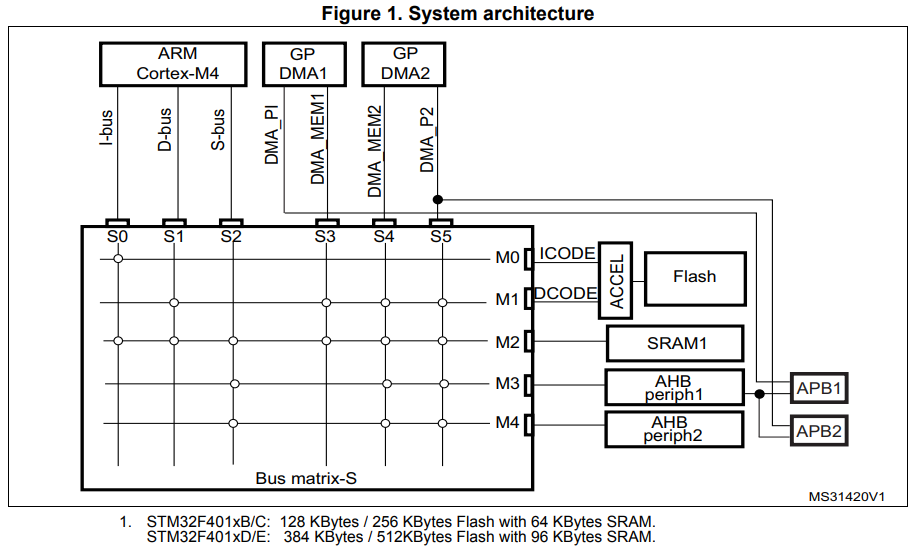
The STM32F401xB/C and STM32F401xD/E feature a 32-bit multilayer AHB bus matrix as their main system. This matrix interconnects:
• Six masters:
– Cortex-M4 with FPU core I-bus, D-bus and S-bus
– DMA1 memory bus
– DMA2 memory bus
– DMA2 peripheral bus
• Five slaves:
– Internal Flash memory ICode bus
– Internal Flash memory DCode bus
– Main internal SRAM
– AHB1 peripherals including AHB to APB bridges and APB peripherals
– AHB2 peripherals
This bus matrix architecture allows masters to access slaves efficiently, enabling concurrent operations when multiple high-speed peripherals work simultaneously. Figure 1 illustrates this architecture.