DMA
DMA- Transfer Properties
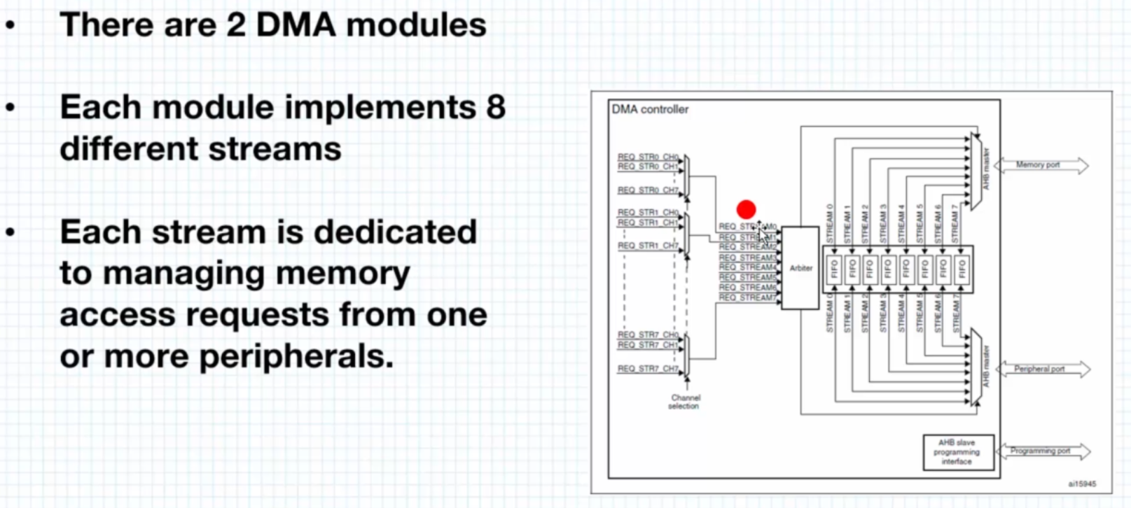
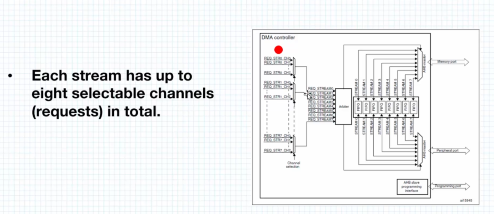
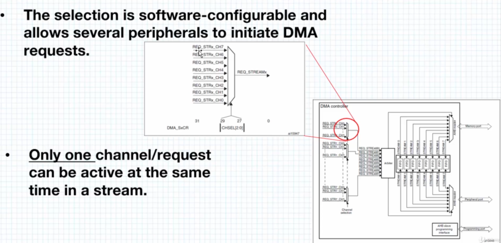
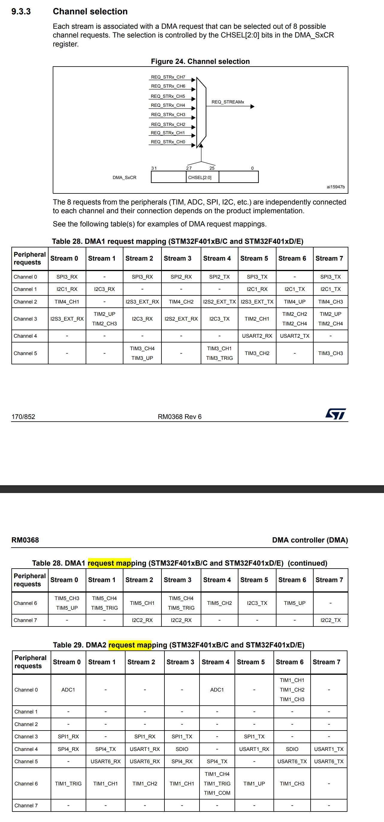
- DMA stream/channel
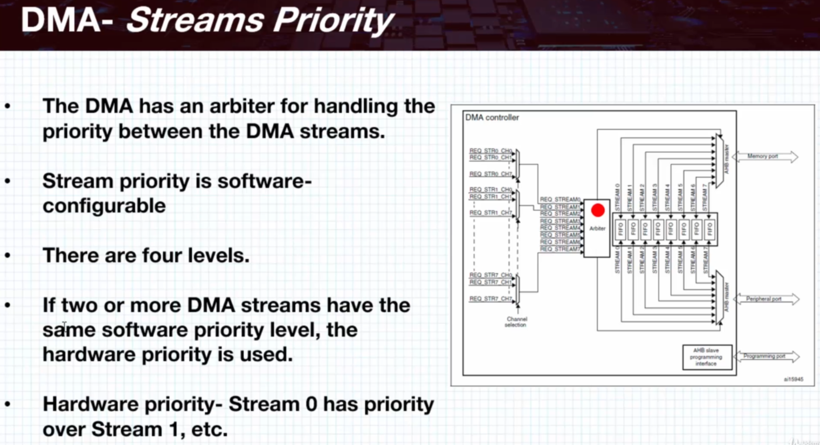
- Stream priority
- Source and destination addresses
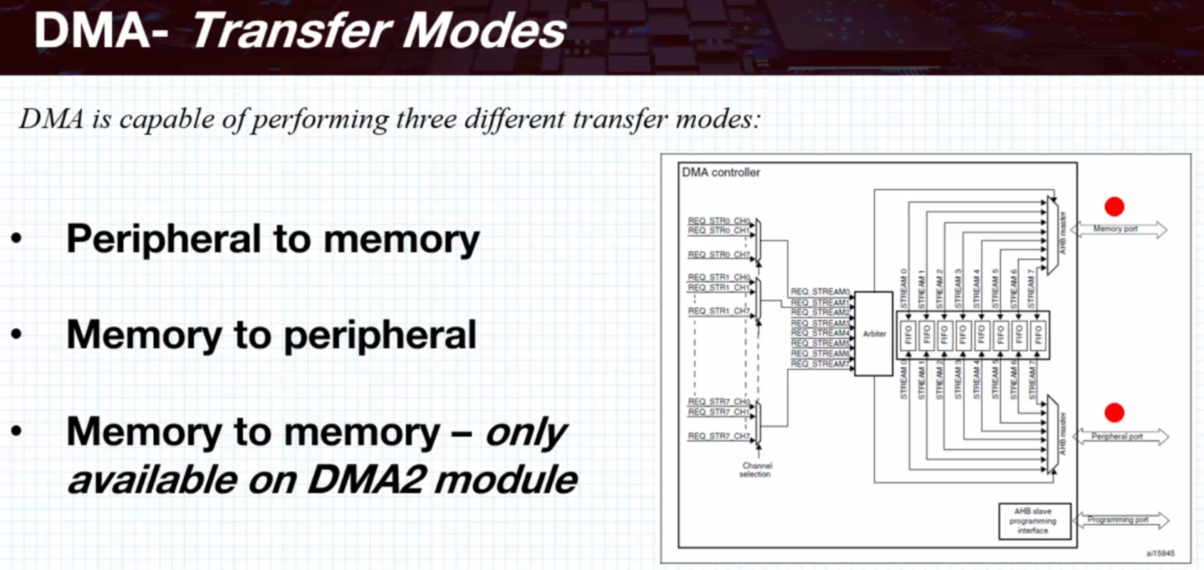
- Transfer mode
- Transfer size
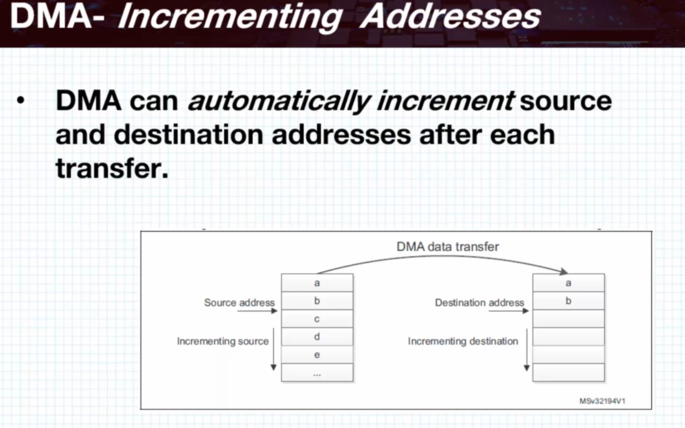
- Source/destination address incrementing or non-incrementing
- Source and destination data width
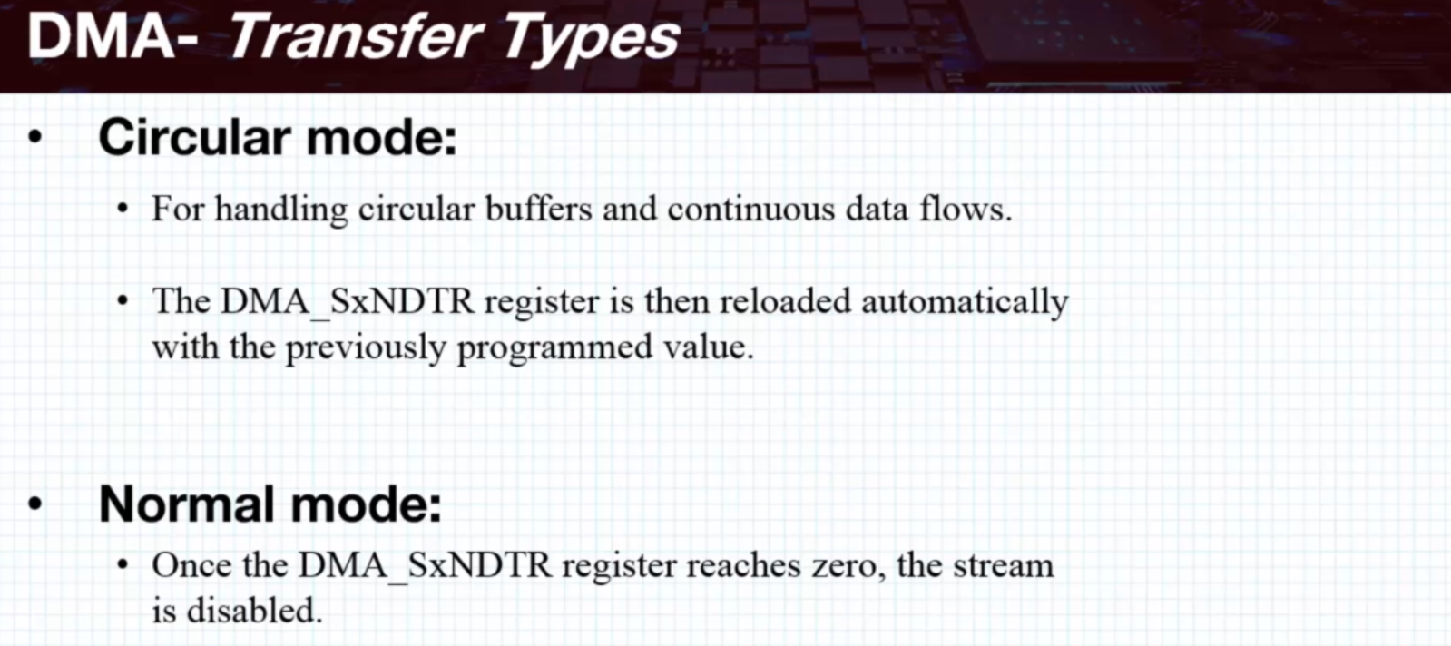
- Transfer type
- FIFO mode
- Source/destination burst size
- Double-buffer mode
- Flow control
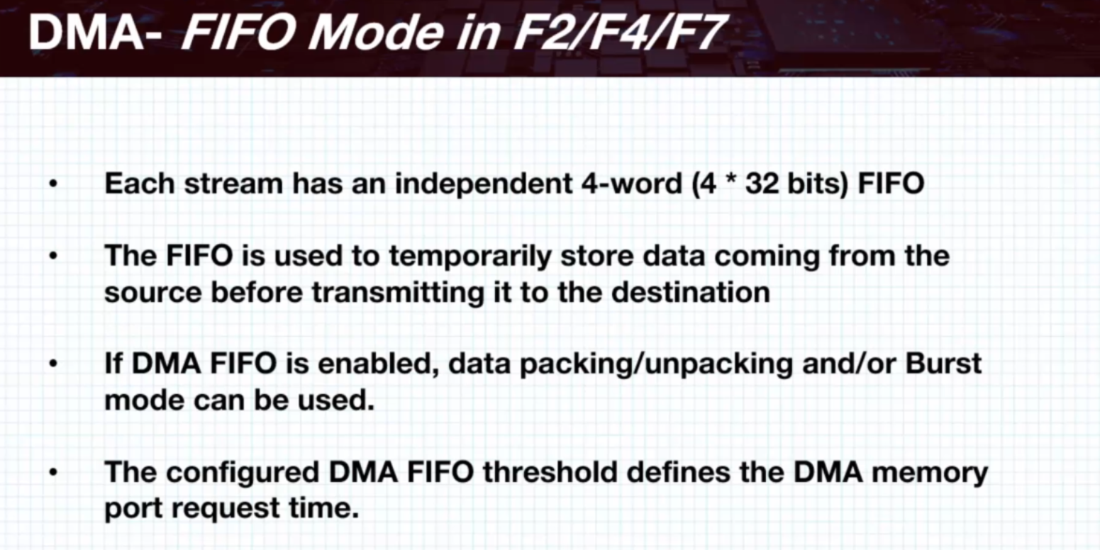
Direct mode: Transfers data directly between source and destination without using FIFO.
FIFO mode: Uses a buffer (FIFO) to manage data transfers.
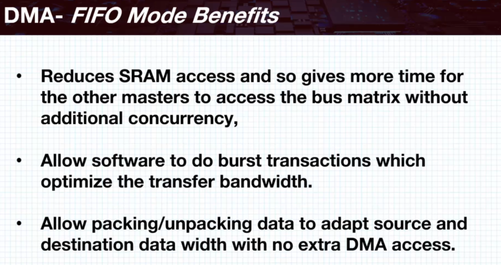
💡 Common DMA modes include:
- Direct mode: Transfers data directly between source and destination without using FIFO.
- FIFO mode: Uses a buffer (FIFO) to manage data transfers.
UART and DMA example
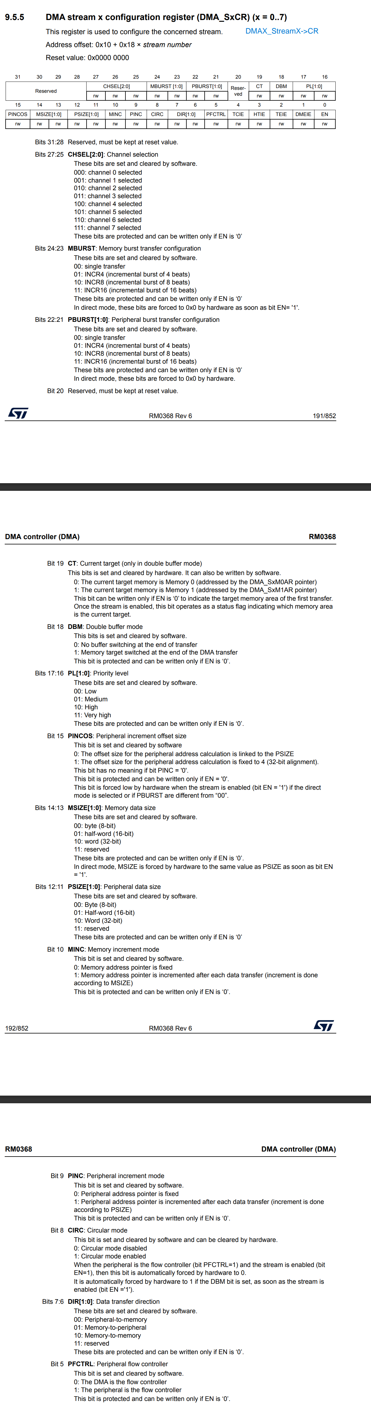
#define DMA1EN              (1U<<21)
#define CHSEL4              (1U<<27)
#define DMA_MEM_INC         (1U<<10)
#define DMA_DIR_MEM_TO_PERIPH (1U<<16)
#define DMA_CR_TCIE         (1U<<4)
#define DMA_CR_EN           (1U<<0)
#define UART_CR3_DMAT       (1U<<7)

void dma1_stream6_init(uint32_t src, uint32_t dst, uint32_t len)
{
    /*Enable clock access to DMA*/
    RCC->AHB1ENR |= DMA1EN;

    /*Disable DMA1 Stream6*/
    DMA1_Stream6->CR &= ~DMA_CR_EN;

    /* Wait untill DMA1 stream 6 is disabled*/
    while(DMA1_Stream6->CR & DMA_CR_EN) {}

    /*Clear all interrupt flags of Stream6*/
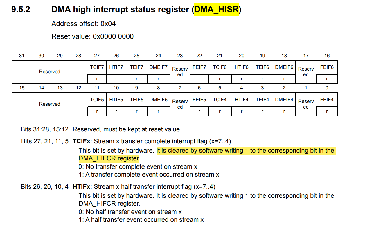
    DMA1->HIFCR |= (1U<<16);
    DMA1->HIFCR |= (1U<<18);
    DMA1->HIFCR |= (1U<<19);
    DMA1->HIFCR |= (1U<<20);
    DMA1->HIFCR |= (1U<<21);

    /*Set the destination buffer*/
    DMA1_Stream6->PAR = dst;

    /*Set the source buffer*/
    DMA1_Stream6->MOAR = src;

    /*Set length*/
    DMA1_Stream6->NDTR = len;

    /*Select Stream6 CH4*/
    DMA1_Stream6->CR = CHSEL4;

    /*Enable memory increment*/
    DMA1_Stream6->CR |= DMA_MEM_INC;

    /*Configure transfer direction*/
    DMA1_Stream6->CR |= DMA_DIR_MEM_TO_PERIPH;

    /*Enable DMA transfer complete interrupt*/
    DMA1_Stream6->CR |= DMA_CR_TCIE;

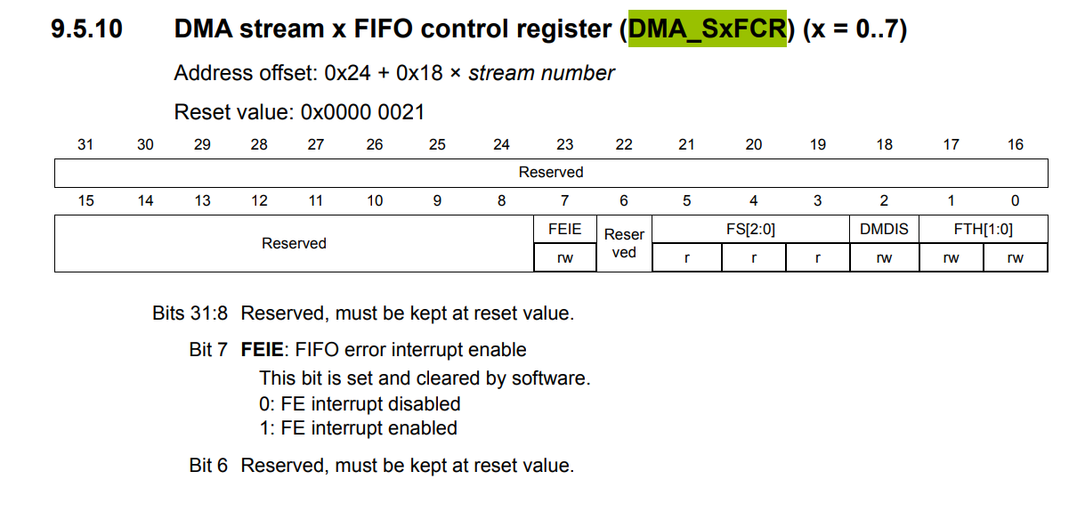
    /*Enable direct mode and disable FIFO*/
    DMA1_Stream6->FCR = 0;

    /*Enable DMA1 Stream6*/
    DMA1_Stream6->CR |= DMA_CR_EN;

    /*Enable UART2 transmitter DMA*/
    USART2->CR3 |= UART_CR3_DMAT;

    /*DMA Interrupt enable in NVIC*/
    NVIC_EnableIRQ(DMA1_Stream6_IRQn);
}

// ...main.c...
#define LED_PIN         GPIOA_5

#define SR_RXNE         (1U<<5)
#define HISR_TCIF6      (1U<<21)
#define HIFCR_CTCIF6    (1U<<21)

static void dma_callback(void)
{
    GPIOA->ODR |= LED_PIN;
}

void DMA1_Stream6_IRQHandler(void)
{
    /*Check for transfer complete interrupt*/
    if(DMA1->HISR & HISR_TCIF6)
    {
        /*Clear flag*/
        DMA1->HIFCR |= HIFCR_CTCIF6;

        /*Do something*/
        dma_callback();
    }
}

static void uart_callback(void);

int main(void)
{
    char message[31] = "Hello from Stm32 DMA transfer\n\r";
    char key;

    /*1.Enable clock access to GPIOA*/
    RCC->AHB1ENR |= GPIOAEN;

    /*2.Set PA5 as output pin*/
    GPIOA->MODER |= (1U<<10);
    GPIOA->MODER &= ~(1U<<11);

    uart2_tx_init(); // you can find this here https://www.notion.so/UART-25bc6bfe6366804f9fa1f089ca2327d9
    dma1_stream6_init((uint32_t) message, (uint32_t)&USART2->DR, 31);

    while(1)
    {
    }
}
DMA mem-to-mem
#define DMAEN              (1U<<22)
#define DMA_SCR_EN         (1U<<0)
#define DMA_SCR_MINC       (1U<<10)
#define DMA_SCR_PINC       (1U<<9)
#define DMA_SCR_TCIE       (1U<<4)
#define DMA_SCR_TEIE       (1U<<2)
#define DMA_SFCR_DMDIS     (1U<<2)

void dma2_mem2mem_config(void)
{
    /*Enable clock access to the dma module*/
    RCC->AHB1ENR |= DMAEN;

    /*Disable dma stream*/
    DMA2_Stream0->CR = 0;

    /*Wait until stream is disabled*/
    while((DMA2_Stream0->CR & DMA_SCR_EN)){}

    /*Configure dma parameters*/

    /*Set MSIZE i.e Memory data size to half-word*/
    DMA2_Stream0->CR |= (1U<<13);
    DMA2_Stream0->CR &= ~(1U<<14);

    /*Set PSIZE i.e Peripheral data size to half-word*/
    DMA2_Stream0->CR |= (1U<<11);
    DMA2_Stream0->CR &= ~(1U<<12);

    /*Enable memory addr increment*/
    DMA2_Stream0->CR |= DMA_SCR_MINC;

    /*Enable peripheral addr increment*/
    DMA2_Stream0->CR |= DMA_SCR_PINC;

    /*Select mem-to-mem transfer*/
    DMA2_Stream0->CR &= ~(1U<<6);
    DMA2_Stream0->CR |= (1U<<7);

		/*Enable transfer complete interrupt*/
    DMA2_Stream0->CR |= DMA_SCR_TCIE;

    /*Enable transfer error interrupt*/
    DMA2_Stream0->CR |= DMA_SCR_TEIE;

    /*Disable direct mode*/
    DMA2_Stream0->FCR |= DMA_SFCR_DMDIS;

    /*Set DMA FIFO threshold*/
    DMA2_Stream0->FCR |= (1U<<0);
    DMA2_Stream0->FCR |= (1U<<1);

    /*Enable DMA interrupt in NVIC*/
    NVIC_EnableIRQ(DMA2_Stream0_IRQn);
}

void dma_transfer_start(uint32_t src_buff, uint32_t dest_buff, uint32_t len)
{
    /*Set peripheral address*/
    DMA2_Stream0->PAR = src_buff;

    /*Set memory address*/
    DMA2_Stream0->M0AR = dest_buff;

    /*Set transfer length*/
    DMA2_Stream0->NDTR = len;

    /*Enable dma stream*/
    DMA2_Stream0->CR |= DMA_SCR_EN;
}

// ...main.c
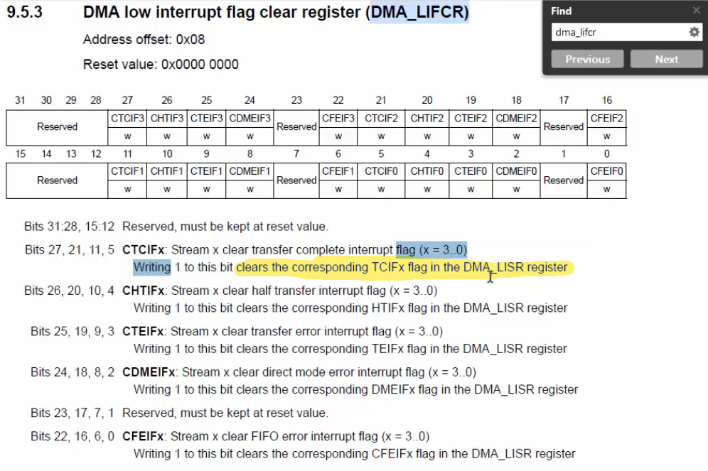
#define LISR_TCIF0        (1U<<5)
#define LIFCR_CTCIF0      (1U<<5)
#define LISR_TEIF0        (1U<<3)
#define LIFCR_CTEIF0      (1U<<3)

#define BUFFER_SIZE 5

uint16_t sensor_data_arr[BUFFER_SIZE] = {892, 731, 1234, 90, 23};
uint16_t temp_data_arr[BUFFER_SIZE];

volatile uint8_t g_transfer_cmplt;

int main(void)
{
		g_transfer_cmplt = 0;

    uart2_tx_init();
    dma2_mem2mem_config();

    dma_transfer_start((uint32_t)sensor_data_arr, (uint32_t)temp_data_arr, BUFFER_SIZE);

    // Wait until transfer complete
    while(!g_transfer_cmplt) {}
		g_transfer_cmplt = 0;

    for (int i = 0; i < BUFFER_SIZE; i++)
    {
        printf("Temp buffer[%d]: %d\r\n", i, temp_data_arr[i]);
    }

    while(1)
    {
    }
}

void DMA2_Stream0_IRQHandler(void)
{
    /*Check if transfer complete interrupt occurred*/
    if((DMA2->LISR) & LISR_TCIF0)
    {
        g_transfer_cmplt = 1;
        /*Clear flag*/
        DMA2->LIFCR |= LIFCR_CTCIF0;
    }

    /*Check if transfer error occurred*/
    if((DMA2->LISR) & LISR_TEIF0)
    {
        /*Do something...*/
        /*Clear flag*/
        DMA2->LIFCR |= LIFCR_CTEIF0;
    }
}
adc dma driver
#define GPIOAEN        (1U<<0)
#define ADC1EN         (1U<<8)
#define CR1_SCAN       (1U<<8)
#define CR2_DMA        (1U<<8)
#define CR2_DDS        (1U<<9)
#define CR2_CONT       (1U<<1)
#define CR2_ADCON      (1U<<0)
#define CR2_SWSTART    (1U<<30)

#define DMA2EN         (1U<<22)
#define DMA_SCR_EN     (1U<<0)
#define DMA_SCR_MINC   (1U<<10)
#define DMA_SCR_PINC   (1U<<9)
#define DMA_SCR_CIRC   (1U<<8)
#define DMA_SCR_TCIE   (1U<<4)
#define DMA_SCR_TEIE   (1U<<2)
#define DMA_SFCR_DMDIS (1U<<2)

#define NUM_OF_CHANNELS 2

uint16_t adc_raw_data[NUM_OF_CHANNELS];

void adc_dma_init(void)
{
    /************GPIO Configuration************/
    /*Enable clock access to ADC GPIO Pin's Port*/
    RCC->AHB1ENR |= GPIOAEN;

    /*Set PA0 and PA1 mode to analog mode*/
    GPIOA->MODER |= (1U<<0);
    GPIOA->MODER |= (1U<<1);
    GPIOA->MODER |= (1U<<2);
    GPIOA->MODER |= (1U<<3);

    /************ADC Configuration************/
    /*Enable clock access to ADC*/
    RCC->APB2ENR |= ADC1EN;

    /*Set sequence length*/
    ADC1->SQR1 |= (1U<<20);
    ADC1->SQR1 &= ~(1U<<21);
    ADC1->SQR1 &= ~(1U<<22);
    ADC1->SQR1 &= ~(1U<<23);

    /*Set sequence*/
    ADC1->SQR3 = (0U<<0) | (1U<<5);

    /*Enable scan mode*/
    ADC1->CR1 = CR1_SCAN;

    /*Select to use DMA*/
    ADC1->CR2 |= CR2_CONT | CR2_DMA | CR2_DDS;

    /************DMA Configuration************/
    /*Enable clock access to DMA*/
    RCC->AHB1ENR |= DMA2EN;

    /*Disable DMA stream*/
    DMA2_Stream0->CR &= ~DMA_SCR_EN;

    /*Wait till DMA is disabled*/
    while((DMA2_Stream0->CR & DMA_SCR_EN)){}

    /*Enable Circular mode*/
    DMA2_Stream0->CR |= DMA_SCR_CIRC;

    /*Set MSIZE i.e Memory data size to half-word*/
    DMA2_Stream0->CR |= (1U<<13);
    DMA2_Stream0->CR &= ~(1U<<14);

    /*Set PSIZE i.e Peripheral data size to half-word*/
    DMA2_Stream0->CR |= (1U<<11);
    DMA2_Stream0->CR &= ~(1U<<12);

    /*Enable memory addr increment*/
    DMA2_Stream0->CR |= DMA_SCR_MINC;

    /*Set periph address*/
    DMA2_Stream0->PAR = (uint32_t)(&(ADC1->DR));

    /*Set mem address*/
    DMA2_Stream0->M0AR = (uint32_t)(&adc_raw_data);

    /*Set number of transfer*/
    DMA2_Stream0->NDTR = (uint16_t)NUM_OF_CHANNELS;

    /*Enable DMA stream*/
    DMA2_Stream0->CR |= DMA_SCR_EN;

    /************ADC Configuration************/
    /*Enable ADC*/
    ADC1->CR2 |= CR2_ADCON;

    /*Start ADC*/
    ADC1->CR2
}
dma timer with adc
#define GPIOAEN        (1U<<0)
#define ADC1EN         (1U<<8)
#define CR1_SCAN       (1U<<8)
#define CR2_DMA        (1U<<8)
#define CR2_DDS        (1U<<9)
#define CR2_CONT       (1U<<1)
#define CR2_ADCON      (1U<<0)
#define CR2_SWSTART    (1U<<30)

#define DMA2EN         (1U<<22)
#define DMA_SCR_EN     (1U<<0)
#define DMA_SCR_MINC   (1U<<10)
#define DMA_SCR_PINC   (1U<<9)
#define DMA_SCR_CIRC   (1U<<8)
#define DMA_SCR_TCIE   (1U<<4)
#define DMA_SCR_TEIE   (1U<<2)
#define DMA_SFCR_DMDIS (1U<<2)

#define NUM_OF_SAMPLES   10
#define NUM_OF_CHANNELS  2

#define TIM2EN          (1U<<0)
#define CR1_CEN         (1U<<0)

uint16_t adc_raw_data[NUM_OF_SAMPLES];

/************** adc_tim_dma_init(void) ***************/
void adc_tim_dma_init(void)
{
    /************** GPIO Configuration ***************/
    /* Enable clock access to ADC GPIO Pin's Port */
    RCC->AHB1ENR |= GPIOAEN;

    /* Set PA0 to analog mode */
    GPIOA->MODER |= (1U<<0);
    GPIOA->MODER |= (1U<<1);

    /************** ADC Configuration ***************/
    /* Enable clock access to ADC */
    RCC->APB2ENR |= ADC1EN;

    /* Select to use DMA */
    ADC1->CR2 |= CR2_DMA|CR2_DDS;

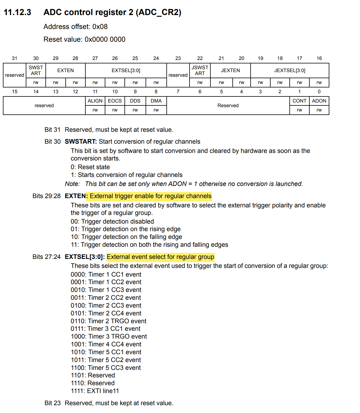
    /* Select external trigger on rising edge */
    ADC1->CR2 |=  (1U<<28);
    ADC1->CR2 &= ~(1U<<29);

    /* Select Timer 2 TRGO event */
    ADC1->CR2 &= ~(1U<<24);
    ADC1->CR2 |=  (1U<<25);
    ADC1->CR2 |=  (1U<<26);
    ADC1->CR2 &= ~(1U<<27);

    /************** DMA Configuration ***************/
    /* Enable clock access to DMA */
    RCC->AHB1ENR |= DMA2EN;

    /*Disable DMA stream*/
    DMA2_Stream0->CR &= ~DMA_SCR_EN;

    /*Wait till DMA is disabled*/
    while((DMA2_Stream0->CR & DMA_SCR_EN)){}

    /*Enable Circular mode*/
    DMA2_Stream0->CR |= DMA_SCR_CIRC;

    /*Set MSIZE i.e Memory data size to half-word*/
    DMA2_Stream0->CR |= (1U<<13);
    DMA2_Stream0->CR &= ~(1U<<14);

    /*Set PSIZE i.e Peripheral data size to half-word*/
    DMA2_Stream0->CR |= (1U<<11);
    DMA2_Stream0->CR &= ~(1U<<12);

    /*Enable memory addr increment*/
    DMA2_Stream0->CR |= DMA_SCR_MINC;

		/*Enable transfer complete interrupt*/
    DMA2_Stream0->CR |= DMA_SCR_TCIE;

    /*Set periph address*/
    DMA2_Stream0->PAR = (uint32_t)(&(ADC1->DR));

    /*Set mem address*/
    DMA2_Stream0->M0AR = (uint32_t)(&adc_raw_data);

    /*Set number of transfer*/
    DMA2_Stream0->NDTR = (uint16_t)NUM_OF_SAMPLES;

    /*Enable DMA interrupt in NVIC*/
    NVIC_EnableIRQ(DMA2_Stream0_IRQn);

    /************** Timer Configuration ***************/
		/* Configure timer period to 100Hz i.e, ADC is going to be sampling at a 100Hz rate, every 10ms */

		/* Enable clock access to TIM2 */
		RCC->APB1ENR |= TIM2EN;

		/* Set TIM prescaler value */
		TIM2->PSC = 16000 - 1;    // 16 000 000 / 16 000 = 1 000

		/* Set TIM auto-reload value */
		TIM2->ARR = 10 - 1;       // 1 000 / 10 = 100Hz

		/* Configure master mode selection bits */
		TIM2->CR2 &= ~(1U<<4);
		TIM2->CR2 |=  (1U<<5);
		TIM2->CR2 &= ~(1U<<6);

		/************** Enable modules ***************/
		/* Enable ADC */
		ADC1->CR2 |= CR2_ADCON;

		/* Enable DMA stream */
		DMA2_Stream0->CR |= DMA_SCR_EN;

		/* Enable Timer */
		TIM2->CR1 |= CR1_CEN;
}

// ...main.c

#define LISR_TCIF0       (1U<<5)
#define LIFCR_CTCIF0     (1U<<5)
extern uint16_t adc_raw_data[NUM_OF_SAMPLES];

volatile uint8_t g_transfer_cmplt;

int main(void)
{
    g_transfer_cmplt = 0;
    uart2_tx_init();
    adc_tim_dma_init();

    while(1)
    {
        if(g_transfer_cmplt)
        {
    g_transfer_cmplt = 0;
            for(int i = 0; i < NUM_OF_SAMPLES; i++)
            {
                printf("Sample number [%d]  = %d \r\n", i, adc_raw_data[i]);
            }
            for(int i = 0; i < 90000; i++){}
        }
    }

}

void DMA2_Stream0_IRQHandler(void)
{
    /*Check if transfer complete interrupt occurred*/
    if((DMA2->LISR) & LISR_TCIF0)
    {
        g_transfer_cmplt = 1;
        /*Clear flag*/
        DMA2->LIFCR |= LIFCR_CTCIF0;
    }

}