SPI
- Synchronous and full-duplex communication between a master and several slave devices.
- Uses two pins for data transfer–SDIN and SDO.
- There is a SCLK pin to synchronize data transfer between two chips.
- There is also a CE pin which is used to initiate and terminate the data transfer.
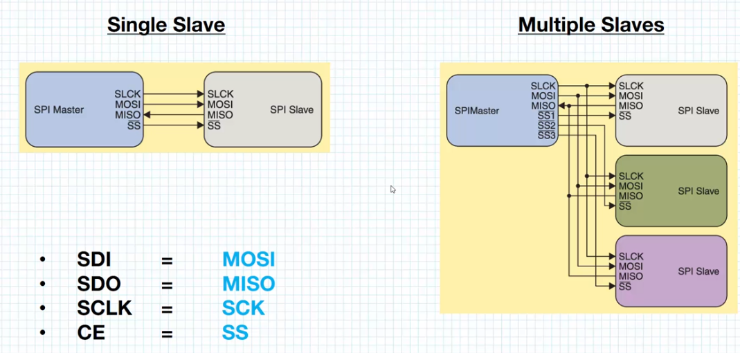
- MOSI: Master Out Slave In, used to send data from master to slave
- MISO: Master In Slave Out, used to send data from slave device to master
- SCK: Serial Clock, used to generate clock to synchronize data transfer between the master and slave device. Generated by master.
- SS: Slave Select, used to select a particular slave in the SPI multiple slaves configuration.
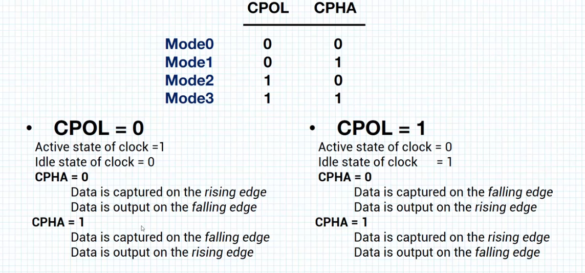
- CPOL = 0 Means sampling on the first edge
- CPOL = 1 Means sampling on the second edge
NSS
-
NSS software mode:
SS line is driven internally by the firmware.
-
NSS hardware mode:
A dedicated GPIO pin is used to drive the SS line.
-
NSS Output Enabled:
Used only when device operates in master mode
-
NSS Output Disabled:
Allows multi-master capability for devices operating in master mode
IT Mode
- NSS hardware mode must be used.
- CPHA and CPOL are forced to conform to Texas Instrument (TI) protocol requirements.
- In this mode NSS signal pulses at the end of every transmitted byte.
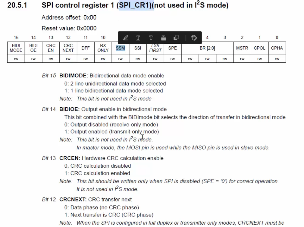
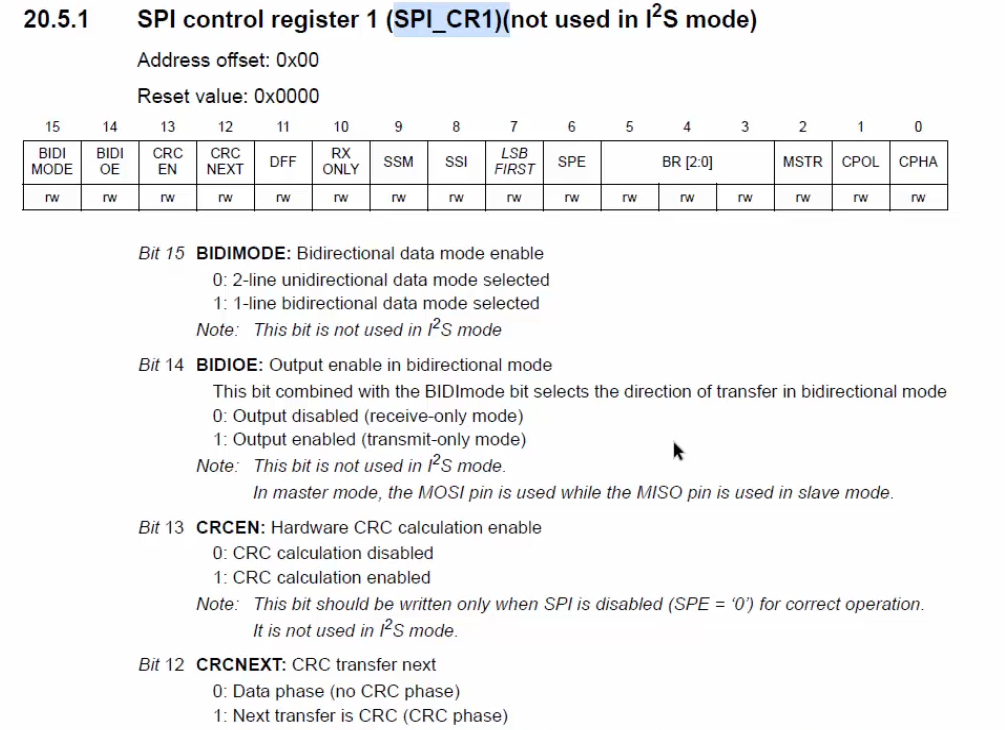
#define GPIOAEN        (1U<<0)
#define SPI1EN         (1U<<12)

#define CR1_SSM        (1U<<9)
#define CR1_SSI        (1U<<8)
#define CR1_MSTR       (1U<<2)
#define CR1_CPOL       (1U<<1)
#define CR1_PHA        (1U<<0)
#define CR2_TXDMAEN    (1U<<1)
#define CR2_RXDMAEN    (1U<<0)
#define CR1_SPE        (1U<<6)

void spi1_dma_init(void)
{
    /************GPIO Configuration************/
    /*Enable clock to PORT of SPI pins*/
    RCC->AHB1ENR |= GPIOAEN;

    /*Set SPI pins mode to alternate function mode*/
    /*PA5*/
    GPIOA->MODER &= ~(1U<<10);
    GPIOA->MODER |=  (1U<<11);

    /*PA6*/
    GPIOA->MODER &= ~(1U<<12);
    GPIOA->MODER |=  (1U<<13);

    /*PA7*/
    GPIOA->MODER &= ~(1U<<14);
    GPIOA->MODER |=  (1U<<15);

    /*PA5*/
    GPIOA->AFR[0] |=  (1U<<20);
    GPIOA->AFR[0] &= ~(1U<<21);
    GPIOA->AFR[0] |=  (1U<<22);
    GPIOA->AFR[0] &= ~(1U<<23);

    /*PA6*/
    GPIOA->AFR[0] |=  (1U<<24);
    GPIOA->AFR[0] &= ~(1U<<25);
    GPIOA->AFR[0] |=  (1U<<26);
    GPIOA->AFR[0] &= ~(1U<<27);

    /*PA7*/
    GPIOA->AFR[0] |=  (1U<<28);
    GPIOA->AFR[0] &= ~(1U<<29);
    GPIOA->AFR[0] |=  (1U<<30);
    GPIOA->AFR[0] &= ~(1U<<31);

    /************SPI Configuration************/
    /*Enable clock access to SPI1 module*/
    RCC->APB2ENR |= SPI1EN;

    /*Set software slave management*/
    SPI1->CR1 |= CR1_SSM | CR1_SSI;

    /*Set SPI to master mode*/
    SPI1->CR1 |= CR1_MSTR;

    /*Set CPHA and CPOL*/
    SPI1->CR1 |= SPI_CR1_BR_0 | CR1_PHA | CR1_CPOL;

    /*Set clock divider : PCLK/4*/
    SPI1->CR1 |=  (1U<<3);
    SPI1->CR1 &= ~(1U<<4);
    SPI1->CR1 &= ~(1U<<5);

    /*Select to use DMA*/
    SPI1->CR2 |= CR2_RXDMAEN | CR2_TXDMAEN;

    /*Enable SPI*/
    SPI1->CR1 |= CR1_SPE;
}

#define DMA2EN          (1U<<22)
#define DMA_SCR_EN      (1U<<0)
#define DMA_SCR_MINC    (1U<<10)
#define DMA_SCR_CIRC    (1U<<8)
#define DMA_SCR_TCIE    (1U<<4)
#define DMA_SCR_TEIE    (1U<<2)
#define DMA_SFCR_DMDIS  (1U<<2)

void dma2_stream3_spi_tx_init(void)
{
  /************DMA Configuration************/
  /*Enable clock access to DMA*/
  RCC->AHB1ENR |= DMA2EN;

  /*Disable DMA stream*/
  DMA2_Stream3->CR = 0;

  /*Wait till DMA is disabled*/
  while((DMA2_Stream3->CR & DMA_SCR_EN)){}

  /*********Configure DMA Stream parameters************/
  /*Enable memory addr increment*/
  DMA2_Stream3->CR |=DMA_SCR_MINC;

  /*Select Channel : CH3*/
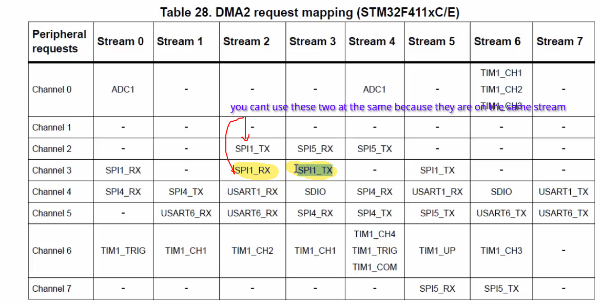
	DMA2_Stream3->CR |= (1U<<25);
	DMA2_Stream3->CR |= (1U<<26);
	DMA2_Stream3->CR &= ~(1U<<27);

  /*Set transfer direction: mem-to-periph*/
  DMA2_Stream3->CR |= (1U<<6);
  DMA2_Stream3->CR &= ~(1U<<7);

  /*Enable transfer complete interrupt*/
  DMA2_Stream3->CR |= DMA_SCR_TCIE;

    /*Enable transfer error interrupt*/
  DMA2_Stream3->CR |= DMA_SCR_TEIE;

  /*Disable direct mode*/
  DMA2_Stream3->FCR =DMA_SFCR_DMDIS;

  /*Set DMA FIFO threshold*/
  DMA2_Stream3->FCR |= (1U<<0);
  DMA2_Stream3->FCR |= (1U<<1);

    /*Enable DMA Stream interrupt in the NVIC*/
      NVIC_EnableIRQ(DMA2_Stream3_IRQn);
}

void dma2_stream2_spi_rx_init(void)
{
  /************DMA Configuration************/
  /*Enable clock access to DMA*/
  RCC->AHB1ENR |= DMA2EN;

  /*Disable DMA stream*/
  DMA2_Stream2->CR = 0;

  /*Wait till DMA Stream is disabled*/
  while((DMA2_Stream2->CR & DMA_SCR_EN)){}

  /*********Configure DMA Stream parameters************/
  /*Enable memory addr increment*/
  DMA2_Stream2->CR |=DMA_SCR_MINC;

  /*Select Channel : CH3*/
	DMA2_Stream2->CR |= (1U<<25);
	DMA2_Stream2->CR |= (1U<<26);
	DMA2_Stream2->CR &= ~(1U<<27);

  /*Set transfer direction : Peripheral to Memory*/
  DMA2_Stream2->CR &=~(1U<<6);
  DMA2_Stream2->CR &=~(1U<<7);

  /*Enable transfer complete interrupt*/
  DMA2_Stream2->CR |= DMA_SCR_TCIE;

  /*Enable transfer error interrupt*/
  DMA2_Stream2->CR |= DMA_SCR_TEIE;

  /*Disable direct mode*/
  DMA2_Stream2->FCR =DMA_SFCR_DMDIS;

  /*Set DMA FIFO threshold : Full*/
  DMA2_Stream2->FCR |= (1U<<0);
  DMA2_Stream2->FCR |= (1U<<1);

  /*Enable DMA Stream interrupt in the NVIC*/
  NVIC_EnableIRQ(DMA2_Stream2_IRQn);
 }


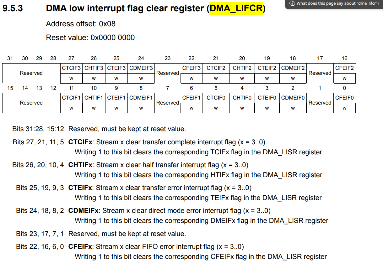
#define LISR_TCIF3      (1U<<27)
#define LISR_TCIF2      (1U<<21)

#define LISR_TEIF3      (1U<<25)
#define LISR_TEIF2      (1U<<19)

#define LIFCR_CTCIF2    (1U<<21)
#define LIFCR_CTCIF3    (1U<<27)

#define LIFCR_CTEIF2    (1U<<19)

void dma2_stream2_spi_receive(uint32_t received_msg, uint32_t msg_len)
{
 /*Clear interrupt flags*/
 DMA2->LIFCR = LIFCR_CTCIF2 | LIFCR_CTEIF2;

 /*Set Peripheral address*/
 DMA2_Stream2->PAR = (uint32_t)(&(SPI1->DR));

 /*Set Memory address*/
 DMA2_Stream2->M0AR = received_msg;

 /*Set transfer length*/
 DMA2_Stream2->NDTR = msg_len;

 /*Enable the DMA Stream*/
 DMA1_Stream2->CR |= DMA_SCR_EN;
}

void dma2_stream3_spi_tranfer(uint32_t msg_to_snd, uint32_t msg_len)
{
 /*Clear interrupt flags*/
 DMA2->LIFCR = LIFCR_CTCIF3 | LIFCR_CTEIF3;

 /*Set Peripheral address*/
 DMA2_Stream3->PAR = (uint32_t)(&(SPI1->DR));

 /*Set Memory address*/
 DMA2_Stream3->M0AR = msg_to_snd;

 /*Set transfer length*/
 DMA2_Stream3->NDTR = msg_len;

 /*Enable the DMA Stream*/
 DMA1_Stream3->CR |= DMA_SCR_EN;
}

void DMA2_Stream3_IRQHandler(void)
{
  if((DMA2->LISR) & LISR_TCIF3)
  {
    //do something...

    //Clear the flag
    DMA2->LIFCR |=LIFCR_CTCIF3;
  }
  else if((DMA2->LISR) & LISR_TEIF3)
  {
    //do something...

    //Clear the flag
        DMA2->LIFCR |=LIFCR_CTEIF3;
  }
}

void DMA2_Stream2_IRQHandler(void)
{
  if((DMA2->LISR) & LISR_TCIF2)
  {
    //do something...

    //Clear the flag
    DMA2->LIFCR |=LIFCR_CTCIF2;
  }
  else if((DMA2->LISR) & LISR_TEIF2)
  {
    //do something...

    //Clear the flag
    DMA2->LIFCR |=LIFCR_CTEIF2;
  }
}