I2C
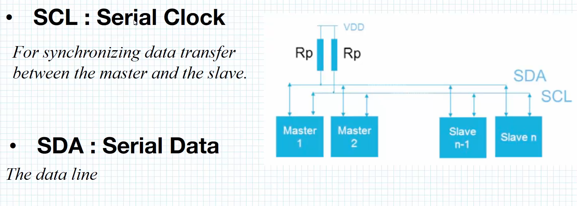
Operation Modes
- Master Transmitter
- Master Receiver
- Slave Transmitter
- Slave Receiver
The Protocol
- Transactions are initiated and completed by the master.
- All messages have an address frame and a data frame.
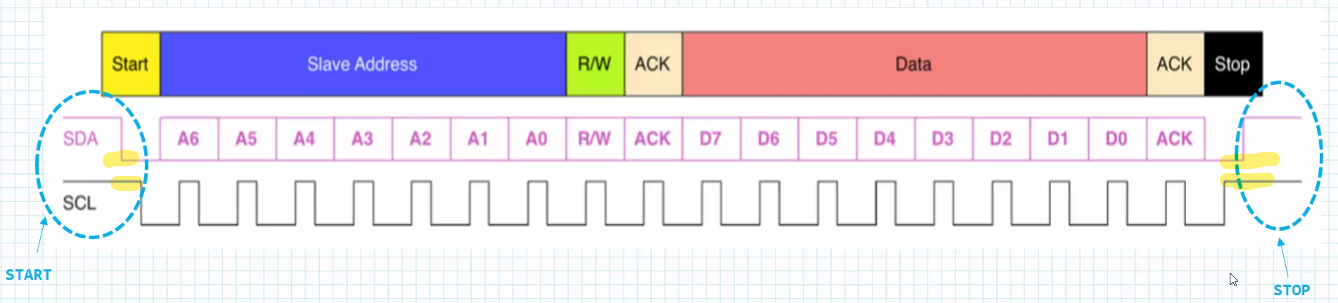
- Data is placed on the SDA line after SCL goes low, and it is sampled after the SCL line goes high.
Start and Stop condition
-
All transactions begin with START and are terminated by STOP
-
A HIGH to LOW transition on the SDA line while SCL is HIGH defines a START condition
-
A LOW to HIGH transition on the SDA line while SCL is HIGH defines a STOP condition.
-
START and STOP conditions are always generated by the master
-
The bus is considered to be free again a certain time after the STOP condition
-
The bus stays busy if a repeated START is generated instead of a STOP condition
-
The address frame is first in any new communication sequence.
-
For a 7-bit address, the address is sent out significant bit (MSB) first, followed by a R/W bit indicating whether this is a read (1) or write (0) operation
-
The data frame begins transmission after the address frame is sent.
-
The master will simply continue generating clock pulses on SCL at a regular interval, and the data will be placed on SDA by either the master or the slave, depending on whether the R/W bit indicated a read or write operation.
I2C Clock Speed
- This is the speed of the I2C interface and should correspond with the bus speeds defined in the I2C specification
The specification defines the following modes :
Standard-mode : 100 KHz max
Fast-mode : 400 KHz max
Fast-mode Plus : 1 MHz
High-speed mode : 3.4 MHz
I2C Duty Cycle
-
Specifies the ratio between tLOW and tHIGH of the I2C SCL line
-
Possible values :
I2C_DUTYCYCLE_2 = 2:1
I2C_DUTYCYCLE_16_9 = 16:9 -
By choosing the appropriate duty cycle we can pre-scale the peripheral clock to achieve the desired I2C speed.
#define GPIOBEN     (1U<<1)
#define I2C1EN      (1U<<21)
#define CR1_SWRST   (1U<<15)
#define CR1_NOSTRETCH (1U<<7)
#define CR1_ENGC      (1U<<6)
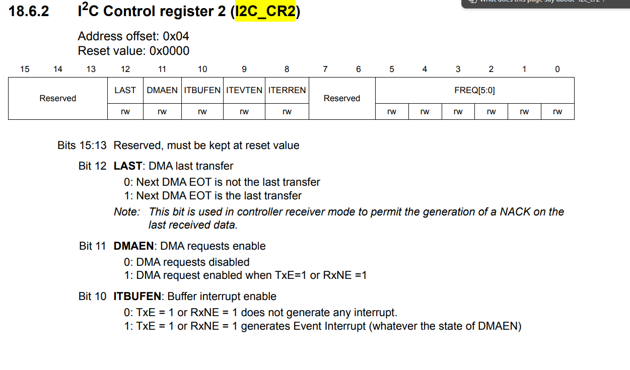
#define CR2_DMAEN     (1U<<11)
#define CR2_LAST      (1U<<12)
#define CR1_PE        (1U<<0)

#define PERIPH_CLK 16

#define I2C_100KHZ 80  // 0B 0101 0000
#define SD_MODE_MAX_RISE_TIME 17

void i2c1_init(void)
{
  /**********I2C GPIO Configuration************/
  /*Enable clock access to GPIOB*/
  RCC->AHB1ENR |= GPIOBEN;

	/*Set PB8 and PB9 mode to alternate function mode*/
	/*PB8*/
	GPIOB->MODER &= ~(1U<<16);
	GPIOB->MODER |= (1U<<17);

	/*Set PB8 and PB9 alternate function type to I2C1 (AF4) */
	/*PB8*/
	GPIOB->AFR[1] &= ~(1U<<0);
	GPIOB->AFR[1] |= (1U<<1);
	GPIOB->AFR[1] |= (1U<<2);
	GPIOB->AFR[1] &= ~(1U<<3);

	/*PB9*/
	GPIOB->AFR[1] &= ~(1U<<4);
	GPIOB->AFR[1] |= (1U<<5);
	GPIOB->AFR[1] |= (1U<<6);
	GPIOB->AFR[1] &= ~(1U<<7);

	/*SCL and SDA respectively*/
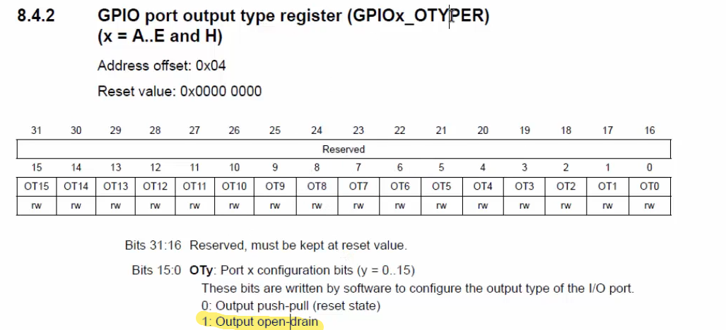
	/*Set output type of PB8 and PB9 to open-drain*/
	GPIOB->OTYPER |= (1U<<8);
	GPIOB->OTYPER |= (1U<<9);

	/**********I2C Configuration************/
	/*Enable clock access to I2C1*/
	RCC->APB1ENR |= I2C1EN;

	/*Reset I2C module*/
	I2C1->CR1 |= CR1_SWRST;

	/*Release the reset*/
	I2C1->CR1 &= ~CR1_SWRST;

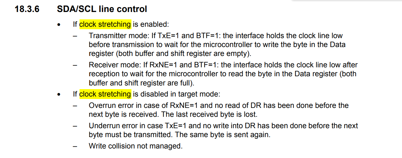
	/*Enable clock stretching*/
	I2C1->CR1 &= ~CR1_NOSTRETCH;

	/*Disable General Call*/
	I2C1->CR1 &= ~CR1_ENGC;

	/*Select to use DMA*/
	I2C1->CR2 |= CR2_DMAEN;

	/*Enable LAST*/
	I2C1->CR2 |= CR2_LAST;

	/*Set source clock speed*/
	I2C1->CR2 |= PERIPH_CLK;

	I2C1->CCR = I2C_100KHZ; /*Based on Computation*/

	I2C1->TRISE = SD_MODE_MAX_RISE_TIME;

	/*Enable I2C module*/
	I2C1->CR1 |= CR1_PE;
}

#define DMA1EN          (1U<<21)
#define DMA_SCR_MINC    (1U<<10)
#define DMA_SCR_TCIE    (1U<<4)

void dma1_stream6_i2c1_tx_init(void)
{
  /*Enable clock access DMA*/
  RCC->AHB1ENR |=DMA1EN;

  /*Select DMA channel : CH1*/
  DMA1_Stream6->CR |= (1U<<25);
  DMA1_Stream6->CR &= ~(1U<<26);
  DMA1_Stream6->CR &= ~(1U<<27);

  /*Enable Mem Addr increment*/
  DMA1_Stream6->CR |= DMA_SCR_MINC;

  /*Enable Transfer Complete Interrupt*/
  DMA1_Stream6->CR |= DMA_SCR_TCIE;

  /*Set Transfer direction : Mem to Periph*/
  DMA1_Stream6->CR |= (1U<<6);
  DMA1_Stream6->CR &= ~(1U<<7);

  /*Enable Stream Interrupt in NVIC*/
  NVIC_EnableIRQ(DMA1_Stream6_IRQn);
}

void dma1_stream5_i2c1_rx_init(void)
{
  /*Enable clock access DMA*/
  RCC->AHB1ENR |=DMA1EN;

  /*Select DMA channel : CH1*/
  DMA1_Stream5->CR |= (1U<<25);
  DMA1_Stream5->CR &= ~(1U<<26);
  DMA1_Stream5->CR &= ~(1U<<27);

  /*Enable Mem Addr increment*/
  DMA1_Stream5->CR |= DMA_SCR_MINC;

  /*Enable Transfer Complete Interrupt*/
  DMA1_Stream5->CR |= DMA_SCR_TCIE;

  /*Set Transfer direction : Periph to Mem*/
  DMA1_Stream5->CR &= ~(1U<<6);
  DMA1_Stream5->CR |= (1U<<7);

  /*Enable Stream Interrupt in NVIC*/
  NVIC_EnableIRQ(DMA1_Stream5_IRQn);
}

void dma1_stream6_i2c1_transfer(uint8_t *msg_to_send, uint32_t msg_len)
{
  if( NULL != msg_to_send )
  {
    /*Clear interrupt flags*/
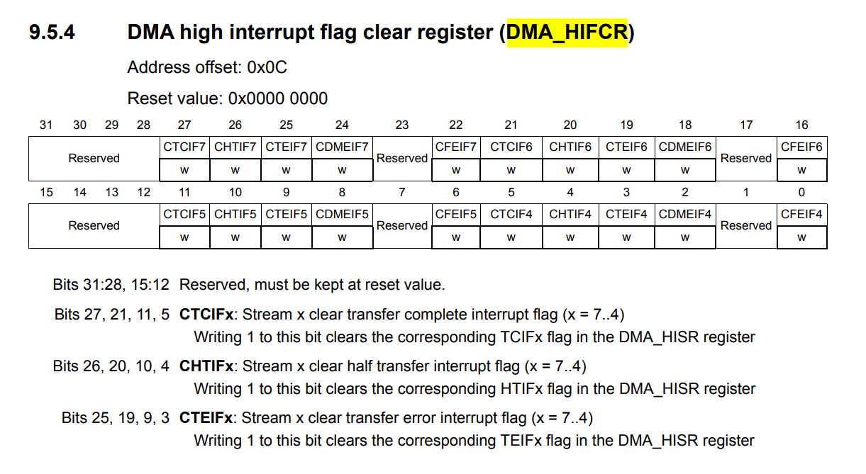
    DMA1->HIFCR = HIFCR_CTCIF5;

    /*Set Peripheral address*/
    DMA1_Stream6->PAR = (uint32_t)(&(I2C1->DR));

    /*Set Memory address*/
    DMA1_Stream6->M0AR = (uint32_t)msg_to_send;

    /*Set transfer length*/
    DMA1_Stream6->NDTR = msg_len;

    /*Enable the DMA Stream*/
    DMA1_Stream6->CR |= DMA_SCR_EN;
  } else
  {
	  // do something
  }
}

void dma1_stream5_i2c1_receive(uint8_t * received_msg, uint32_t msg_len)
{
  if( NULL != received_msg )
  {
    /*Clear interrupt flags*/
    DMA1->HIFCR = HIFCR_CTCIF5;

    /*Set Peripheral address*/
    DMA1_Stream5->PAR = (uint32_t)(&(I2C1->DR));

    /*Set Memory address*/
    DMA1_Stream5->M0AR = (uint32_t)received_msg;

    /*Set transfer length*/
    DMA1_Stream5->NDTR = msg_len;

    /*Enable the DMA Stream*/
    DMA1_Stream5->CR |= DMA_SCR_EN;
  }
  else
  {

  }
}

#define CR1_START   (1U<<8)
#define SR1_SB      (1U<<0)
#define SR1_ADDR    (1U<<1)
#define SR1_TXE     (1U<<7)
#define CR1_ACK     (1U<<10)
#define SR1_BTF     (1U<<2)
#define CR1_STOP    (1U<<9)

void i2c_dma_read(uint8_t slave_addr, uint8_t reg_addr, uint8_t *p_read_buff, uint16_t num_of_bytes)
{
    /*Wait while BUSY flag is set*/
    while((I2C1->SR2 & SR2_BUSY)){}

    /*Generate START condition*/
    I2C1->CR1 |= CR1_START;

    /*Wait until the SB flag to be set*/
    while(!(I2C1->SR1 & SR1_SB)){}

		/* clear flags (according to the documentation)*/
    /*Read SR1*/
    I2C1->SR1;

    /*Send Slave Addr "Write"*/
    I2C1->DR = (slave_addr<<1|0);

    /*Wait for Addr Flag to be set*/
    while(!((I2C1->SR1)& SR1_ADDR)){}

		/* clear flags (according to the documentation)*/
    /*Read SR1*/
    I2C1->SR1;
    /*Read SR2*/
    I2C1->SR2;

    /*Wait for TXE flag to be set*/
    while(!(I2C1->SR1 & SR1_TXE)){}

    /*Send RegAddr*/
    if(num_of_bytes >= 2)
    {
        /*Enable ACK*/
        I2C1->CR1 |= CR1_ACK;
    }
    else
    {
        /*Disable ACK*/
        I2C1->CR1 &=~CR1_ACK;
	  }

    /*Send register address to read*/
    I2C1->DR = reg_addr;

    /*Wait for BTF flag*/
    while(!(I2C1->SR1 & SR1_BTF)){}

    /*Generate RESTART*/
    I2C1->CR1 |= CR1_START;

    /*Wait until the SB flag to be set*/
    while(!(I2C1->SR1 & SR1_SB)){}

    /*Read SR1*/
    I2C1->SR1;

    /*Send Slave Addr with "read"*/
    I2C1->DR = (slave_addr<<1|1);

    /*Wait for the Addr flag to be set*/
    while(!((I2C1->SR1)& SR1_ADDR)){}

    /*Call DMA receive function*/
    dma1_stream5_i2c1_receive(p_read_buff, num_of_bytes);

    /*Read SR1*/
    I2C1->SR1;

    /*Read SR2*/
    I2C1->SR2;
}

void i2c_dma_write(uint8_t slave_addr, uint8_t *p_write_buff, uint16_t num_of_bytes)
{
    /*Wait while BUSY flag is set*/
    while((I2C1->SR2 & SR2_BUSY)){}

    /*Generate START condition*/
    I2C1->CR1 |= CR1_START;

    /*Wait until the SB flag is set*/
    while(!(I2C1->SR1 & SR1_SB)){}

    /*Read SR1*/
    I2C1->SR1;

    /*Send Slave Addr "Write"*/
    I2C1->DR = (slave_addr<<1|0);

    /*Wait for Addr Flag to be set*/
    while(!(I2C1->SR1 & SR1_ADDR)){}

    /*Call DMA transfer function*/
    dma1_stream6_i2c1_transfer(p_write_buff, num_of_bytes);

    /*Read SR1*/
    I2C1->SR1;

    /*Read SR2*/
    I2C1->SR2;
}

void DMA1_Stream6_IRQHandler(void)
{
    if((DMA1->HISR) & HISR_TCIF6)
    {
        //do_ssomething

        /*Generate Stop*/
        I2C1-> =| CR1_STOP;

        /*Clear the flag*/
        DMA1->HIFCR |= HIFCR_CTCIF6;
    }
}

void DMA1_Stream5_IRQHandler(void)
{
    if((DMA1->HISR) & HISR_TCIF5)
    {
        //do_ssomething

        /*Generate Stop*/
        I2C1-> =| CR1_STOP;

        /*Clear the flag*/
        DMA1->HIFCR |= HIFCR_CTCIF5;
    }
}